Electron microscopes
Our electron microscope suite includes two scanning electron microscopes and two transmission electron microscopes.

The electron microscope suite at Victoria University of Wellington consists of two scanning electron microscopes and two transmission electron microscopes, as well as various tools for sample preparation. These preparation tools include carbon, platinum, gold and other sample coaters, and an ion beam thinner.
Scanning electron microscopes
JEOL 6500F
The JEOL 6500F is a superior instrument for use in nanotechnology, materials science and biology. This field emission scanning electron microscope offers high resolution as well as a high stability and current, in a small spot size. It also offers the ability to generate high x-ray fluxes, enabling chemical analysis at high resolution conditions.
The instrument is fitted with a Gatan cryo unit for examination of biological samples and other hydrated materials by stabilising them under the beam at a low temperature. The unit also allows the fracture of materials which are soft at room temperature - exposing their internal microstructure and enabling the analysis of components and phases in systems such as emulsions and suspensions.
The specifications for the JEOL 6500F are:
- Resolution: ~ 5.0 nm
- Magnification: 10x-500,000x
- Image modes: secondary electron image (SEI) and backscattered electron image (BEI)
- Energy dispersive spectroscopy (EDS) and elemental mapping capability
- Acceleration voltage: 0.5-30 kV
- Specimen size: up to 150 mm in diameter
- 5 axis motor stage control: x, y, z, tilt.
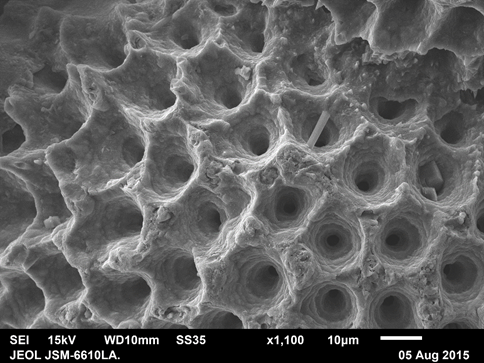
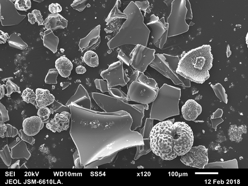
Jeol JSM-6610LA variable vacuum SEM
- Resolution~8nm
- For Micron scale work and analysis, SEM can image non-conductive “uncoated” samples due to the variable vacuum capability.
- Acceleration /Voltages 0.5 – 30kV.
- Magnification x10 – x500,000.
- Equipped with tungsten emitter.
- A dry Silicon drift EDS detector for Elemental Analysis and Mapping.
- An Backscatter Electron Detector for use with Compositional imaging and Topological imaging
- An Robinson RCJ-6610 8.6 FC Cathodluminescence detector for Geological samples
- 5-axis motorised stage control: x, y, z and tilt.
Transmission electron microscope
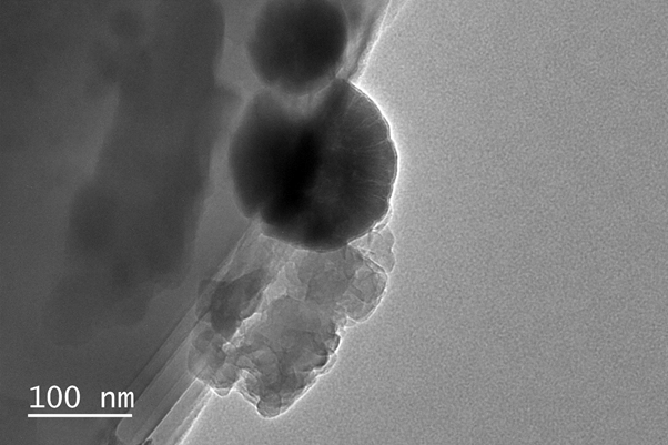
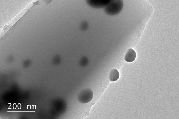
Jeol JEM-2100F—our highest-resolution TEM
- For nano-scale work and analysis
- Equipped with a Heated Schottky Field Emission emitter
- Resolution:~ 0.15 nm
- Magnification x10 – x1.500,000
- Acceleration voltage of 200 kV
- Specimen tilt range +- 25 degrees
- A dry Silicon Drift EDS detector for elemental analysis and mapping of samples
- A STEM system equipped with both bright field and dark field detectors for use with STEM imaging and EDS mapping
- A Gatan diffraction camera for capturing electron diffraction patterns off samples
- A Gatan high-resolution camera capable of collecting conventional images on its high-resolution CCD camera with a resolution of 1024 x 1024 pixels.
JEOL 2010
The JEOL 2010 transmission electron microscope (TEM) is a high-resolution analytical microscope that is mainly used for materials research and the study of nanoparticulate samples. Its superior point-to-point resolution of 0.15 nm makes this instrument ideal for imaging samples on the atomic scale.
The instrument is capable of conventional, dark field, and high-resolution TEM as well as energy-dispersive spectroscopy, selected area electron diffraction, nanobeam diffraction, and convergent-beam diffraction.
The microscope is equipped with both a plate camera and a digital camera. The digital camera is a Gatan Peltier cooled CCD camera fitted below the viewing chamber, making low intensity, high resolution, real-time imaging and filming possible.
In addition to regular single- and double-tilt holders, a heating stage holder and a beryllium double-tilt holder (for optimised EDS analysis) are available.
The specifications of the JEOL 2010 are:
- Resolution: ~0.15 nm
- Magnification: 10x-8,000,000x
- Energy dispersive spectroscopy (EDS) capability
- Acceleration voltage: 200 kV
- Specimen tilt range: ± 25°
- CCD camera resolution: 1024 x 1024 pixels.
We welcome enquiries for users of the facility. All enquiries from potential users should contact:

Electron Microscopy Technician
School of Chemical and Physical Sciences