Equipment
Lithography
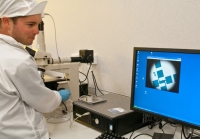
Karl Suss MJB3 mask aligner
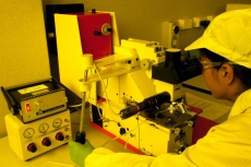
The Karl Suss MJB3 will be familiar to those with experience in lithography and is a great place to start for new students and researchers. The alignment uses a manual process, which means that users are required to become experienced in the intricacies of good alignment. The MJB3 is capable of 2 µm resolution when used correctly.
Masks and resist
Masks can be created at the NEST Laboratory and users are expected to provide their own masks. The MJB3 takes 4-inch mask plates.
We have a campus-wide software licence for LayoutEditor to allow users to design their own masks. There is a small selection of useful contact geometries and gratings currently available here.
We use the AZ series AZ 1518 as our standard resist and have a small stock of the image reversal AZ 5214. We also have microchemical SU8 in-house. If users require other resists, they may be brought into the cleanroom.
Developers, substrate treatment chemicals and resist removers are also available here.
Metallisation and dielectric deposition
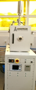
Angstrom engineering evaporator
The Angstrom engineering evaporator has two thermal evaporation sources. It is suitable for the deposition of metals such as Al, Au and Ag. Both sources have an INFICON rate deposition controller which enables the creation of very accurate film thicknesses, but co-deposition is not possible. The rotating substrate holder is suitable for samples up to four inches in diameter. Users are required to bring their own shadow mask if required, and frequent users should provide their own boats and deposition materials.
Note: we do not have e-gun evaporation capabilities at present.
Ezzi Vision sputter coater
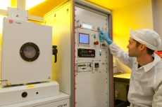
The HHV sputter coater by Ezzi Vision has a single source RF magnetron sputter deposition target. The system is capable of depositing both metals and dielectrics, including Ti, Ag, Ni, SiO2 and ZnO at present. The system comes equipped with an INFICON rate deposition controller for high accuracy of film thicknesses. Frequent users will be required to provide their own 3-inch diameter source material.
Etching
Oxford Instruments Plasmalab 80
Reactive ion etching is a common process in microelectronics to carve patterns into silicon or any other substrate material. At present we have Ar, O2 and SF6 gas for etching. Whether your material can be etched with this system will depend on the gases available and the selectivity between your substrate material and any standard mask. Determining the etch recipe takes time, so users should add this to their expected experimental time.
Although we do not have a list of standard recipes, there is a wealth of etching experience in the team. We are happy to help, advise and in need collaborate with our colleagues at other sites via the MacDiarmid Institute.
Wet etching
This is currently unavailable, but there is space in non-clean areas of the School for wet-etch processing.
Inspection
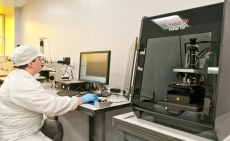
Dektak profilometer
We have a Dektak in the cleanroom. This tool is essential for inspecting metal layer thicknesses, resist and etch profiles and sample surfaces. It is quick and simple to use and allows immediate verification of a process.
Nikon 66 optical microscope
We use a Nikon optical microscope with digital camera to inspect samples during processing runs.
Device characterisation
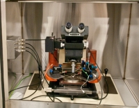
Rucker and Rolls 666 probe station
The probe station is set up with four high precision Ti probes on micromanipulators and is housed in a custom-made Faraday box with a high quality co-axial cable running to the micromanipulator. The probe station is equipped with a vacuum chuck and objective lenses of various magnification for maximum flexibility. Users are encouraged to buy their own tips for non-standard samples.
Agilent 4156C
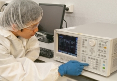
The Agilent 4156C (Precision Semiconductor Parameter Analyser) is connected to the probe station and comes equipped with four high-resolution source measure units (SMUs) capable of femtoamp resolution. Kelvin probe measurements are possible and nA measurements of nanowire devices are considered routine. The 4156C is also capable of quasi CV measurements. Full details of the capabilities can be found on the Agilent website and users are encouraged to read the manual before using the instrument. It will however be familiar to those who have used previous models in the range.
Gold bonder
A gold ball miller is available. Users are required to bring their own chip packaging material.
Sample preparation
Plasma etch
The Plasma Etch has both Ar and O2 gas supplies. This desktop system offers substrate cleaning and surface treatment with a dry process, which is particularly useful for PDMS (polydimethylsiloxane) and other flexible substrate preparations. The procedure is quick - pump down takes only a few minutes and the process time depends on the user. A 20 s O2 plasma treatment for example, is a very useful step post-lithography and prior to lift-off as a cleaner substrate results in better material adhesion. Users are asked to consult the cleanroom manager before loading materials into the system.
Wet bench and substrate cleaning
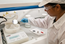
We have two fume hoods each equipped with a spin coater. One coater is designated for use with photoresist only and the other is for polymer deposition and sample trials.
Hot plates, ultrasonic baths, basic lab glassware and solvents are readily available.