Cryogenic memory research
Among the most pressing new challenges in quantum computing is the need for reliable memory that can operate at cryogenic temperatures.
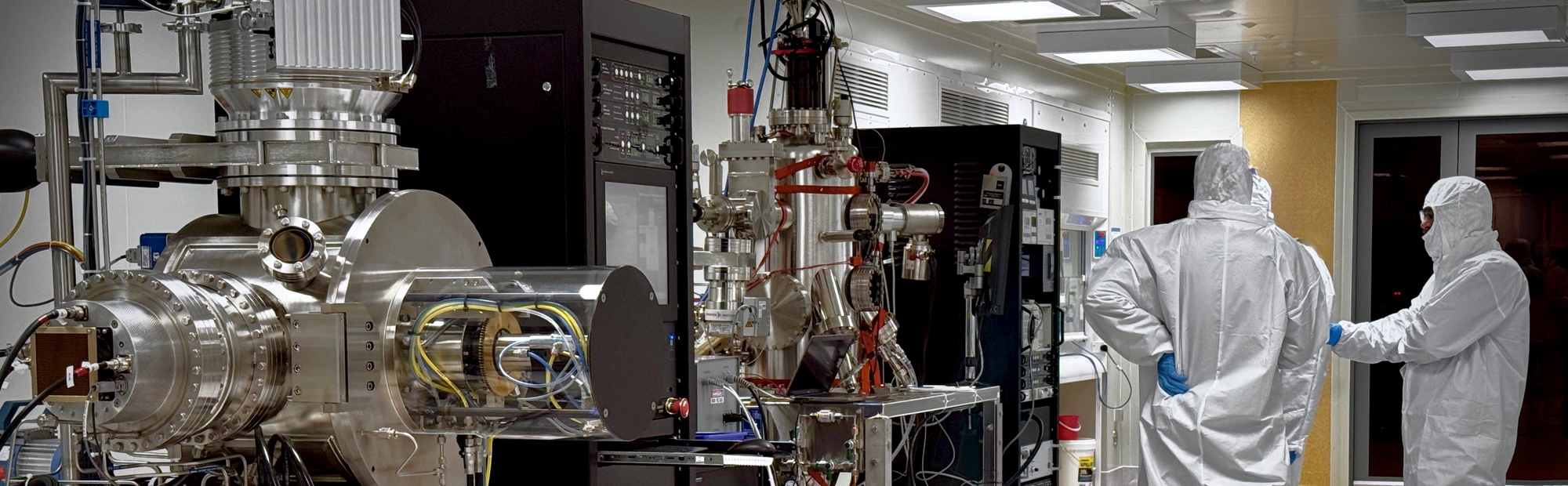
As quantum computing systems grow in complexity, new challenges emerge around scaling the supporting electronics. Among the most pressing is the need for reliable memory that can operate at cryogenic temperatures—conditions required by superconducting qubits and logic circuits. In a joint project between Paihau—Robinson Research Institute and the School of Chemical and Physical Sciences, we are developing cryogenic memory solutions that can meet this demand, based on nearly two decades of research into rare-earth nitride materials.
The science
Our approach centres on rare-earth nitrides—magnetic semiconductors with finely tunable properties. Materials such as gadolinium nitride (GdN) and samarium nitride (SmN) are used to fabricate multilayer magnetic structures that store data in their magnetisation state. These structures are engineered so that one magnetic layer remains fixed while the other can be switched using a small magnetic field or a spin-polarised current.
These memory devices function reliably at temperatures below -269 °C, making them ideal for integration within the cryogenic environment of a quantum processor. Each bit occupies the area of a single superconducting Josephson junction, enabling dense, scalable memory arrays. Because the same materials and fabrication processes are used for both the memory and the logic circuits, integration is straightforward. The switching mechanism is energy-efficient, requiring only minimal external stimulus.
Impact and potential
Conventional memory systems are not well-suited to cryogenic operation, limiting current efforts to scale superconducting and quantum computing systems. Our cryogenic memory technology addresses this limitation directly, offering a practical pathway to embedding memory on the cold stage close to the quantum processor.
This development enables lower-latency data storage and reduces the need for the bulky control cables connecting the quantum chip to room-temperature electronics—a major bottleneck in today’s architectures. Our goal is to scale our devices to a memory array prototype that demonstrates speed, efficiency, and seamless compatibility with superconducting digital logic. While not intended for mass-market applications, these devices offer a vital solution for specialised, low-temperature computing environments. Our ultimate goal is to show our memory scaling to a density above 100 Mbit/cm2, critical for companies like IBM and Google to achieve their quantum computing technology roadmaps.
In parallel, the research is generating protected intellectual property and laying the foundation for a small-scale, New Zealand-based manufacturing capability focused on superconducting components for quantum electronics.
Collaboration and partners
This work is a joint initiative between Paihau–Robinson Research Institute and the School of Chemical and Physical Sciences (SCPS) at Te Herenga Waka—Victoria University of Wellington. The programme is led by Dr Simon Granville and SCPS’s Prof Ben Ruck, supported by the New Zealand Government’s Endeavour Fund.
International collaboration plays a crucial role. Our team is working with research groups and companies in Japan, the United States, Italy, and Australia to refine materials, validate fabrication techniques, and test scalability. These partnerships ensure that our innovations can be quickly adapted for real-world deployment and integrated into global superconducting computing systems.
Our cryogenic memory research reflects New Zealand’s leadership in advanced materials science and its growing role in shaping the future of quantum technologies.